- Joined
- Mar 9, 2017
- Messages
- 27,221
- Reaction score
- 19,608
- Location
- Ontario, Canada
- Gender
- Male
- Political Leaning
- Progressive
???
Ummm....never mind.
You obviously don't understand what I said.
Bye.
lol... why not explain, then, bud? I'm all ears.
")

???
Ummm....never mind.
You obviously don't understand what I said.
Bye.
AMD Zen 5 CPUs are made with TSMC's N4X node.Tsmc is the only one getting good yields at the most advanced nodes.
Intel is having TSMC make their CPUs now.Samsung has poor yields at anything below 4 nm, and Intel is a good generation behind Samsung to my understanding
I'm not going to pay it, either. I'll find other alternatives...or I just won't buy it. That means the manufacturer loses sales, which means they lose money.
Like Trump says, "They are going to come in because it's good for them to come in."
Intel CPUs are made in Taiwan by TSMC.Which means they need to find a solution that doesn't mean they are affected by the tariffs.
Someone will have to make their chips somewhere other than Taiwan.Intel CPUs are made in Taiwan by TSMC.
Apple CPUs are made in Taiwan by TSMC.
AMD CPUs are made in Taiwan by TSMC.
Nvidia graphics cards are made in Taiwan by TSMC.
AMD graphics cards are made in Taiwan by TSMC.
What alternative are you envisioning here?
How will they do that? TSMC is the company with the lithography machines to make them, and the only company that makes those lithography machines already has more than five years of backorders.Someone will have to make their chips somewhere other than Taiwan.
shrug...How will they do that? TSMC is the company with the lithography machines to make them, and the only company that makes those lithography machines already has more than five years of backorders.
I suppose that people in the United States could simply stop buying computers and smartphones.shrug...
I don't know, but they'll have to figure out a way or they are going to lose a lot of sales.

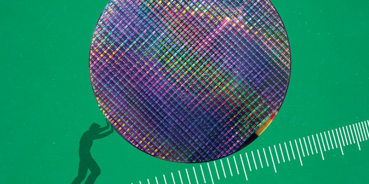
Trump To Tariff Chips Made In Taiwan, Targeting TSMC
The tariffs would ensnare cutting-edge smartphone and PC-related chips for Apple, AMD and Nvidia if enacted. But Trump is betting his plan will bring more chip production to the US.www.pcmag.com
MAGA voters, do you have ****ing idea how utterly ****ing stupid this is? Like totally mind-blowing stupid.
You voted for it.
Trump had a plan a few months ago, that I didn't think much of at the time, but maybe he was onto something.
US chipmaking nears death: Intel warns it may give up on cutting-edge chips
Intel warns it may halt development of its 14A chip, signaling an end to US chipmaking dominance and increasing reliance global leaders like TSMC.www.businessinsider.com
Yes. Their last two revolutionary leaps forward in CPU design came in 2006 and 2011.Intel is in deep doodoo
Trump had a plan a few months ago, that I didn't think much of at the time, but maybe he was onto something.
His idea was for a company that would license TSMC manufacturing processes, make chips in the United States, and be co-owned by five different tech companies (TSMC, Apple, Nvidia, Broadcom, and Qualcomm).
Yes. Their last two revolutionary leaps forward in CPU design came in 2006 and 2011.
They had plans for a new revolutionary leap forward in CPU design, but then they could only afford to do either it or their new foundry processes, but not both, so they scrapped their work on the new CPU concepts and laid off the engineering team that was working on it to focus on their foundry processes.
I wonder, if they are now abandoning their foundry processes, will they try to resurrect their now-scrapped CPU design and rehire the engineers who were developing it?
It will be better than nothing if Intel folds.Taiwan has restricted TSMC on what it can build in the US, so TSMC can't produce the most advanced nodes in the US
It will be better than nothing if Intel folds.
I think that Trump's plan for this new company plans on it acquiring Intel's foundries.Intel will likely sell its foundries or spin it off like AMD did with global foundries.
I can't see Intel folding. They have a habit of making comebacks.It will be better than nothing if Intel folds.
Economies of scale are not in intels favorI can't see Intel folding. They have a habit of making comebacks.
I have a hard time grasping that they are working at the angstrom levels now. When I was in CMP, the 1 micron boundary was just broken. We got down to 0.12 microns when I left the industry.
They aren't, actually. Those are marketing nanometers, not engineering nanometers.I have a hard time grasping that they are working at the angstrom levels now.
They aren't, actually. Those are marketing nanometers, not engineering nanometers.
What TSMC calls 3nm, Samsung calls 2nm, and Intel calls 18a, are actually the 7nm node in real world engineering measurements.
Any idea why? I wonder if the 18a is how flat they have to keep the chip for process resolution?They aren't, actually. Those are marketing nanometers, not engineering nanometers.
What TSMC calls 3nm, Samsung calls 2nm, and Intel calls 18a, are actually the 7nm node in real world engineering measurements.
They will be stuck on the 7nm node for a little while, but they will probably eventually achieve the 5nm node, probably when they start using High-NA Extreme Ultraviolet Lithography.Which I think is likely the limit of how small the features can be considering atoms are 0.1 to 0.5 nm in size.
They had to change transistor design so that it was no longer a two dimensional design. Below a certain size the two dimensional transistors stopped working. They had to switch to a 3D design. So they had to start estimating transistor size instead of directly measuring it.It's been more than 2 decades for me knowing the latest in the field. We went by line widths. Not nodes. Could the node size be the transistor region instead of the line widths?
I had another thought about that. We actually do not have too many nodes left to go before we can't go any smaller.Taiwan has restricted TSMC on what it can build in the US, so TSMC can't produce the most advanced nodes in the US
This isn't what I was speaking of. The transisters always took more width, and I believe we were doing 3D back then. I mean this was the that they could resolve to. It was used for the traces between transistors.They had to change transistor design so that it was no longer a two dimensional design. Below a certain size the two dimensional transistors stopped working. They had to switch to a 3D design. So they had to start estimating transistor size instead of directly measuring it.
This isn't what I was speaking of. The transisters always took more width, and I believe we were doing 3D back then. I mean this was the that they could resolve to. It was used for the traces between transistors.
 spectrum.ieee.org